CMOS Inverter & Clocked CMOS Logic Circuit Design
Overview
Final project for EE 251 (Digital Circuits) at West Virginia University. Designed a CMOS inverter and multi-input logic circuit. Simulated in LTSpice to study how transistor sizing affects voltage transfer curves and noise margins. The project progressed from a basic inverter to a fully optimized clocked CMOS circuit implementing A+BC.
What I Did
- Simulated a CMOS inverter with a PMOS sizing of L = 10 µm and analyzed its voltage transfer curve and noise margins.
- Designed a CMOS logic circuit implementing the complement of A+BC using series/parallel NMOS and PMOS networks.
- Optimized transistor W/L ratios across multiple simulation runs to balance NMH and NML within a 0.15 V threshold.
- Extended the design into a clocked CMOS circuit with a precharge transistor, footer transistor, and output inverter.
Procedure
The proejct had three parts plus a bonus part. In the first part, a normal inverter circuit was created with an unoptmized W/L ratio. The noise margins were calculated by exporting the IV characteristic data from LTspice into Excel. To find the noise margins, the slope needs to be calculated, using Vin / Vout. After calculating the slope for each data point, slopes of -1 were found. These points indicated the VIH, VIL, VOH, and VOL Using these numbers you can get the NML and NMH with the equations, NMH = VOH - VIH and NML = VIL - VOL. This process was iterated on for each circuit to optimize the noise margins for the standard CMOS inverter, the logic circuit, and the clocked CMOS circuit.
Built With
Diagrams & Pictures
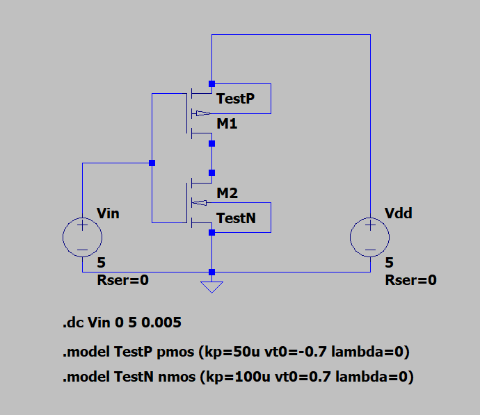
CMOS Inverter Schematic
1 / 4