Simple 8-Bit CPU
Overview
Final project for my digital logic lab (CPE 271L) at West Virginia University. Starting from a provided VHDL template with the ALU, RAM, MUX, and registers already built, I completed the Program Counter, designed the Control Unit, and wired everything together into a working 8-bit CPU on a DE10-Lite FPGA. The finished processor supports three instructions (load, add, and store) and executes them through a multi-state fetch, decode, and execute cycle driven entirely by the clock signal.
What I Did
- Implemented the Program Counter's increment logic in VHDL using a variable and the := assignment operator.
- Diagrammed the full CPU datapath, labeling every connection with the signal names used in the VHDL (cuToMarLoad, pcToMarMux, irOut, marToRamReadAddr, and others).
- Wrote out the STOREA sequence in plain English, then mapped the Fetch, LOADA, ADDA, and STOREA sequences to enumerated states in the Control Unit's finite state machine.
- Transcribed the finite state machine into VHDL case statements, defining which control signals go high or low and which ALU opcode is active at each state.
- Instantiated and connected every component in a top-level entity through port mapping, following the CPU diagram.
- Verified correct operation in the Quartus waveform simulator, confirming the clk, aOut, irOut, pcOut, and increment signals as the CPU ran entirely off the clock with no external inputs.
How It Works
How the CPU works can be visualized by the finite state machine diagram below. The CPU fetches the first instruction from memory by loading the first address into the memory address register (MAR). The CPU then fetches the data at the address loaded into the MAR and loads it into the memory data register in (MDRI). The op code from the data (the three most significant bits) is decoded by the control unit (CU).
The CU enables certain components of the CPU based on the op code. The three op codes that the CPU supports are LOADA, ADDA, and STOREA. The LOADA operation takes the value at a specified address and loads it into the accumulator. ADDA adds the value at a specified address to the value in the accumulator by bitwise addition. STOREA stores the value of the accumulator into memory at a specified address.
Built With
Diagrams & Pictures
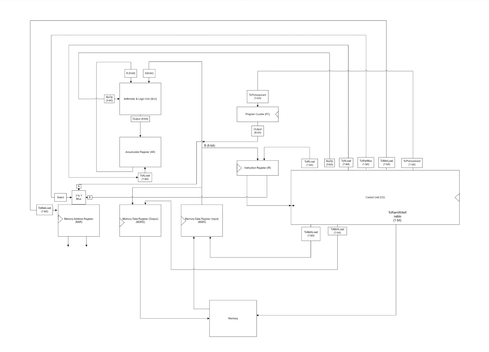
CPU Datapath Block Diagram
1 / 3